Our Services
From quick-turn prototypes to advanced multilayer production — transparent pricing and engineering support at every stage.
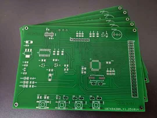
2-Layer Prototype Service
Our classic 1.6mm prototype board. Green solder mask, ENIG finish, and three copies included — ideal for getting ideas onto your bench fast.
- 1oz copper on both layers, 6mil trace/space
- ENIG (gold) finish, lead-free and RoHS compliant
- 3 copies included, order in multiples of three
- Ships in 9–12 calendar days
4 & 6-Layer Service
More layers for improved RF performance, better power distribution and denser routing. Built to IPC-6012 Class 2 standards with X-ray verification.
- 4 or 6 copper layers, 1.6mm standard thickness
- Controlled impedance available with test report
- Blind and buried vias on request
- Ships in 9–14 calendar days
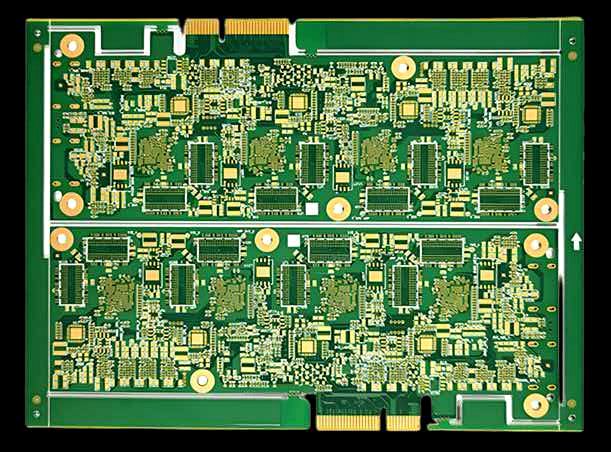
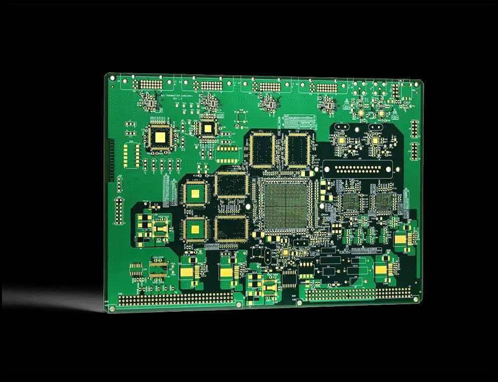
HDI & Fine-Pitch
For compact, high-performance designs: micro-vias, via-in-pad, and fine-pitch BGA breakout. Manufactured with laser drilling and sequential lamination.
- Micro-vias down to 0.1mm, HDI stack-ups up to 3+N+3
- Via-in-pad (VIPPO), filled and plated
- Fine trace/space down to 3mil/3mil
- Ships in 12–18 calendar days
More capabilities
Flex & Rigid-Flex
Polyimide flex circuits and rigid-flex combinations for space-constrained and moving assemblies.
Super Swift
Need it yesterday? Our expedited service ships prototypes in 4–5 business days.
Assembly (PCBA)
Turnkey component sourcing and SMT assembly — get fully populated boards from one partner.