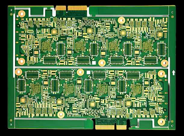
A good stack-up is the foundation of a manufacturable, reliable PCB. Get it right and routing becomes easier, signals stay clean, and the board performs as simulated. Get it wrong and you're looking at cost overruns, EMI headaches, and possibly a full redesign.
Start with the signal layers
The single most important rule: every signal layer should be adjacent to a solid reference plane. This gives return currents a low-impedance path, which reduces crosstalk and electromagnetic interference. For a 4-layer board, a common stack is Signal / GND / VCC / Signal — both signal layers reference a plane.
Symmetry is your friend. Arrange layers mirror-symmetrically around the board centre to prevent warping during reflow.
Balance the copper
Uneven copper distribution causes the board to bend during the high temperatures of reflow soldering. Keep the copper density roughly equal on both sides of the stack. If one side is sparse, add copper pour (ground fill) to balance it out. This is one of the cheapest fixes for a host of assembly problems.
Plan impedance up front
If your design involves high-speed signals — USB, HDMI, DDR, RF — controlled impedance isn't optional. Tell your fabricator your target impedance and stack-up early; trace width is a function of dielectric thickness, dielectric constant, and copper weight. Attempting to hit 50Ω after the fact usually means a redesign.
What to send your fabricator
- Layer count and order (top to bottom)
- Board thickness and material (e.g. FR-4, 175Tg)
- Any controlled-impedance nets and their targets
- Copper weight per layer
Don't guess — ask
Every fab house has slightly different materials and capabilities. Before you lock in a stack-up, send it to your manufacturer for review. At MPCB, this DFM review is free and included with every quote. A five-minute conversation can save weeks of rework.